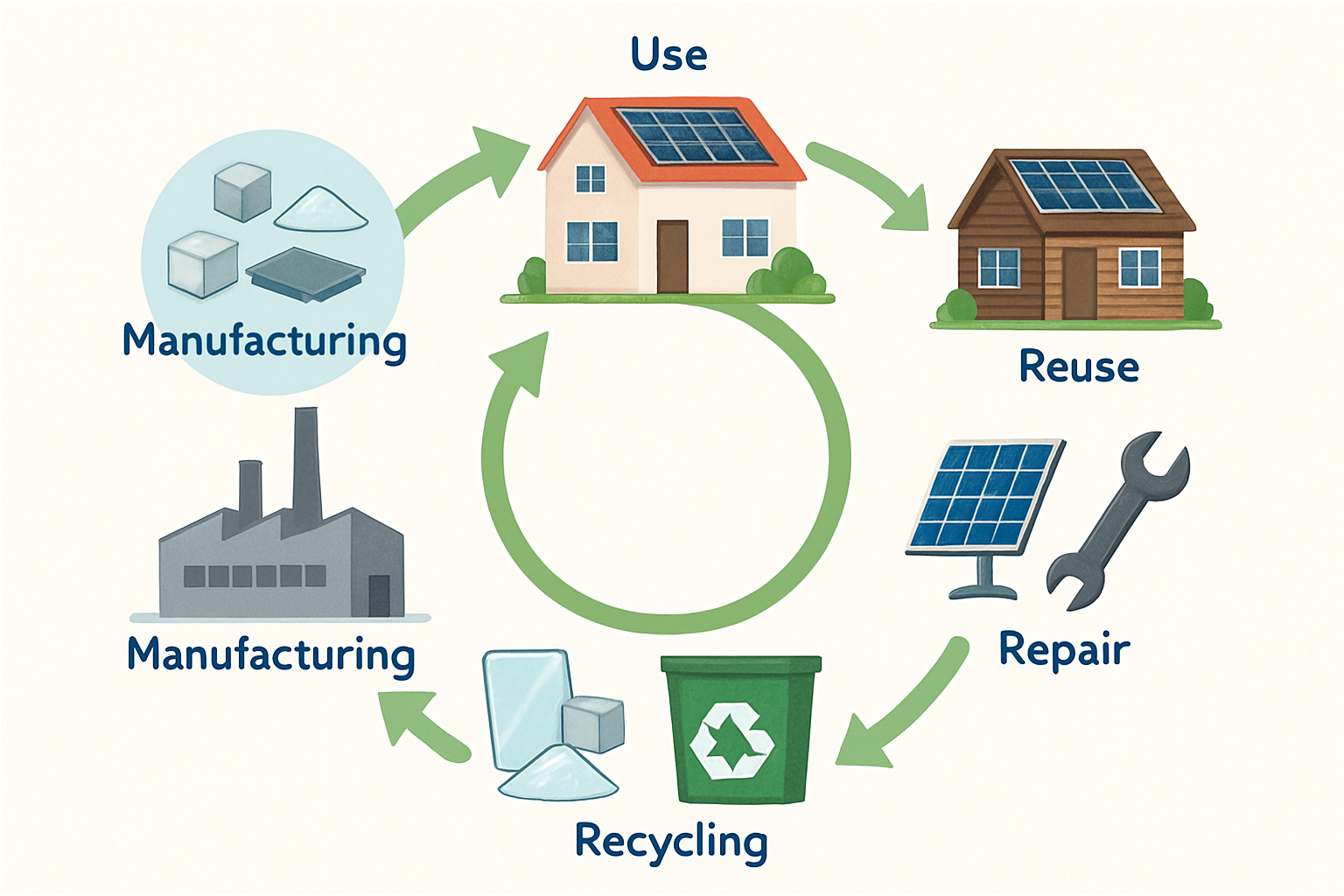
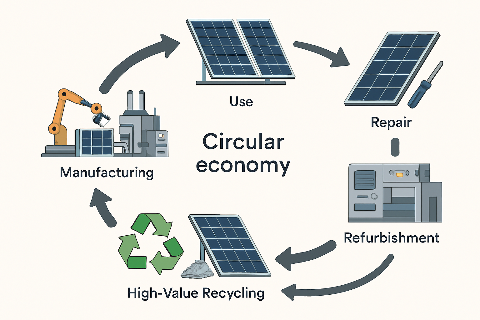
The solar industry is at the forefront of the clean energy transition. As installations scale up globally, the question of what happens to panels at the end of their life becomes critical. Building a circular economy—where materials are reused and recycled rather than discarded—is essential for long-term sustainability. The two dominant technologies, crystalline silicon (c-Si) and thin-film, present different challenges and opportunities for circularity. This analysis compares them to determine which is better positioned for a sustainable future.
Understanding the Material Composition
The materials inside a solar module directly influence its recyclability, economic value, and environmental impact. Crystalline silicon and thin-film technologies have fundamentally different constructions.
The Anatomy of a c-Si Module
Crystalline silicon modules are the most common type on the market, accounting for over 95% of global production according to the International Energy Agency (IEA). Their construction involves several key materials. High-purity silicon wafers form the heart of the solar cells. These cells are connected by copper and silver wiring and then laminated between layers of glass and a protective polymer backsheet, all held together in a sturdy aluminum frame. The value of these modules at end-of-life is largely tied to the aluminum, copper, silver, and increasingly, the silicon itself. As noted in the IEA's Solar PV Global Supply Chains report, recovering high-purity silicon and silver can make recycling a profitable business.
The Makeup of Thin-Film Modules
Thin-film modules, primarily Cadmium Telluride (CdTe) models, use a different approach. Instead of silicon wafers, a very thin layer of semiconductor material is deposited directly onto a glass substrate. A second pane of glass then encapsulates it. This design uses significantly less semiconductor material and eliminates the need for a bulky aluminum frame. While this reduces the overall material intensity, it does involve critical materials like tellurium and a hazardous element, cadmium. However, the cadmium is locked in a stable compound, minimizing risk during operation.
| Component | Crystalline Silicon (c-Si) | Thin-Film (CdTe) |
|---|---|---|
| Primary Semiconductor | High-Purity Silicon | Cadmium Telluride (CdTe) |
| Frame | Aluminum | Typically Frameless |
| Front Cover | Glass | Glass |
| Back Cover | Polymer Backsheet | Glass |
| Key Conductors | Silver, Copper | Various thin metal layers |
| Weight per m² | ~12-15 kg | ~10-12 kg |
The Recycling Process: A Tale of Two Technologies
The distinct material stacks of c-Si and thin-film modules necessitate different end-of-life processing methods. Each has developed specialized techniques to maximize material recovery.

Deconstructing Crystalline Silicon Panels
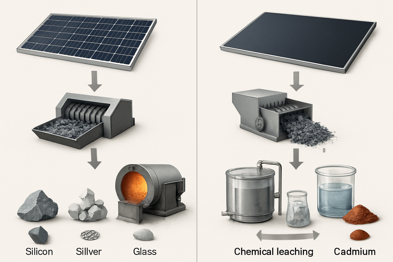
Recycling c-Si modules is a multi-step process. First, the aluminum frame and junction box are removed manually. The remaining laminate is then shredded. A thermal process called pyrolysis is often used to burn away the polymer encapsulants at high temperatures, which helps to separate the silicon cells from the glass. Further mechanical and chemical processing can then isolate valuable materials like copper, silver, and silicon. The main challenge lies in achieving the high purity required for these materials to be reintroduced into new solar modules, though the Solar PV Global Supply Chains report suggests that recovering 85% of solar-grade silicon and other high-value materials is achievable.
Reclaiming Materials from Thin-Film Panels
Thin-film module recycling is primarily a chemical process. After shredding the entire module, the crushed material is subjected to a leaching process where acids dissolve the semiconductor film from the glass surfaces. The dissolved metals, including cadmium and tellurium, can then be precipitated and separated with high efficiency—often over 95%. This allows for a closed-loop system where the recovered semiconductor material can be directly used to manufacture new modules. The glass cullet is also recovered and can be used in other industrial applications.
Evaluating Circularity: Beyond Recycling Rates
A true measure of solar module circularity goes beyond simple material recovery rates. It includes economic feasibility, potential for reuse, and the overall environmental footprint from manufacturing to disposal.
Economic Viability and Material Value
The business case for recycling differs significantly between the two technologies. For c-Si, profitability is sensitive to the market prices of silver and silicon. As manufacturers continue to reduce the amount of silver in cells to cut costs, the economic incentive for recycling could diminish. In contrast, thin-film recycling is often integrated directly into the manufacturing process by the producers. This creates a secure, internal supply chain for critical materials like tellurium and provides a strong economic driver for high collection and recovery rates.
Lifespan, Degradation, and Reuse Potential
Crystalline silicon panels have a long history of field performance, with lifespans often exceeding 30 years. This proven durability has created a growing secondary market for used modules, particularly for off-grid energy storage systems. Reusing panels extends their functional life, which is a core principle of the circular economy. Thin-film modules also have long lifespans, but their reuse market is less developed. This is partly due to a more diverse range of module sizes and electrical specifications, making standardization for second-life applications more complex.
Carbon Footprint and Energy Payback Time
Circularity also considers the environmental impact of production. Manufacturing high-purity silicon for c-Si modules is an energy-intensive process. As a result, c-Si panels generally have a higher initial carbon footprint and a longer energy payback time (EPBT) than thin-film modules. The less energy-intensive deposition process for thin-film gives it an advantage in this area, contributing positively to its overall lifecycle sustainability.
The Path Forward for a Circular Solar Industry
Ultimately, the advancement of the silicon photovoltaic circular economy and the thin-film photovoltaic circular economy depends on industry-wide innovation and supportive policies.
Design for Disassembly
The future of solar panel recycling circularity lies in module design. Manufacturers of both c-Si and thin-film panels are exploring new designs that make it easier to separate materials at the end of life. This includes using non-permanent adhesives or developing encapsulants that can be dissolved without high heat, reducing the cost and complexity of recycling.
Policy and Producer Responsibility
Regulatory frameworks are crucial drivers. Extended Producer Responsibility (EPR) schemes, which make manufacturers responsible for the end-of-life collection and treatment of their products, are essential for ensuring high recycling rates. These policies create a level playing field and provide the financial certainty needed to invest in advanced recycling infrastructure for all module types.
A Nuanced Picture, Not a Single Winner
So, which module wins the circularity race? The answer is not straightforward. Crystalline silicon benefits from a massive installed base, high-value recoverable materials, and a growing reuse market. Its primary challenge is the complexity and cost of separating its intertwined materials. Thin-film technology excels with a highly efficient, closed-loop recycling process that recovers nearly all of its semiconductor material. Its hurdles include managing a hazardous material (albeit safely) and developing a more robust secondary market. Rather than a single winner, the future is a multi-faceted approach where both technologies improve, driven by smart design, supportive policy, and a shared commitment to a sustainable energy future.
Frequently Asked Questions
Which solar panel is more recyclable?
Both types are highly recyclable, but the processes and recovered materials differ. Thin-film (CdTe) recycling can recover over 90% of semiconductor material for use in new modules. Crystalline silicon recycling focuses on recovering glass, aluminum, copper, and increasingly, high-purity silicon and silver.
Is the cadmium in thin-film solar panels dangerous?
The cadmium is in a stable compound (Cadmium Telluride) and is encapsulated between glass layers, posing minimal risk during operation. End-of-life management through established recycling programs is crucial to prevent environmental release.
Can I reuse old c-Si solar panels?
Yes, a secondary market for used c-Si panels is growing. These panels can be used in off-grid applications or in areas with lower efficiency requirements. Proper testing is essential to ensure safety and performance.


Leave a comment
All comments are moderated before being published.
This site is protected by hCaptcha and the hCaptcha Privacy Policy and Terms of Service apply.