An inverter is the heart of any solar energy system, but its performance is deeply tied to temperature. When an inverter gets too hot, it enters a protective state called derating, reducing its power output to prevent damage. While many focus on external cooling, the most effective solution lies in the initial design phase: engineering an efficient thermal path. This involves creating a clear, low-resistance route for heat to travel from its source to the outside environment, ensuring the inverter operates at its full potential.
Understanding Heat Transfer in Power Inverters
An effective thermal management strategy begins with a solid grasp of how heat moves. In power electronics, heat transfer occurs in three primary ways, and managing them all is crucial for creating an efficient thermal path.
The Three Modes of Heat Transfer
Heat flows from hotter areas to cooler ones through conduction, convection, and radiation. In an inverter, conduction moves heat from a semiconductor chip to its casing and then to a heat sink. Convection takes over as airflow, either natural or fan-assisted, carries the heat away from the heat sink. Finally, radiation releases thermal energy as electromagnetic waves from the surfaces of the components and enclosure. A failure in any of these stages can create a thermal bottleneck.
Identifying Key Heat Sources
The primary sources of heat within an inverter are the power semiconductors, such as Insulated Gate Bipolar Transistors (IGBTs) or Metal-Oxide-Semiconductor Field-Effect Transistors (MOSFETs). These components generate heat due to switching and conduction losses during the DC-to-AC conversion process. Other significant heat sources include magnetic components like transformers and inductors, as well as capacitors. Pinpointing these hot spots is the first step in designing a path for their thermal energy to escape.
Defining the Thermal Path
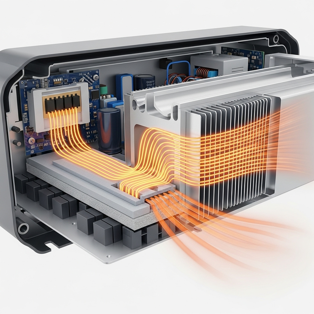
A thermal path is the complete journey heat takes from the semiconductor junction where it is generated to the ambient air outside the inverter. This path includes the semiconductor material itself, the thermal interface material (TIM), the heat sink, and the enclosure. Each step adds thermal resistance; the goal of thermal path engineering is to minimize the total resistance to allow for maximum heat dissipation.
Component-Level Thermal Design Strategies
Preventing derating starts at the micro-level with careful component selection and circuit board layout. Decisions made here have a cascading effect on the entire system's thermal performance.

Selecting Thermally Efficient Components
The first line of defense is to generate less heat. This is achieved by selecting semiconductors with low on-resistance (RDS(on)). Components like Silicon Carbide (SiC) MOSFETs often offer higher efficiency and generate less waste heat compared to traditional silicon counterparts, reducing the overall thermal load. As the Clean Energy Innovation report from the IEA notes, efficiency improvements in power electronics are a continuous driver of innovation.
The Critical Role of Thermal Interface Materials (TIMs)
Even perfectly flat surfaces have microscopic air gaps that trap heat and impede conduction. Thermal Interface Materials (TIMs)—such as thermal pastes, pads, and greases—are applied between a heat-generating component and its heat sink to fill these gaps. A high-quality TIM with low thermal resistance is essential for creating an unbroken and efficient path for heat to conduct away from the semiconductor.
PCB Layout for Optimal Heat Dissipation
The Printed Circuit Board (PCB) itself can be engineered to be an active part of the thermal solution. Techniques include using heavy copper pours (planes) to spread heat laterally, placing thermal vias to transfer heat from the top of the board to the bottom, and strategically positioning hot components to avoid concentrating heat in one area. This turns the entire board into a preliminary heat spreader.
System-Level Thermal Path Engineering
Once component-level design is optimized, the focus shifts to the macroscopic system. This includes the heat sink that does the heavy lifting and the enclosure that facilitates the final heat exchange with the environment.
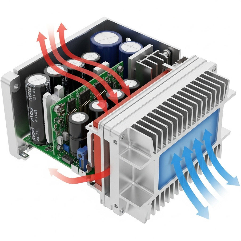
Heat Sink Design and Optimization
The heat sink is the primary component for dissipating concentrated heat into the surrounding air. Its effectiveness depends on several factors:
| Design Factor | Impact on Performance |
|---|---|
| Material | Aluminum is common due to its good thermal conductivity and low weight. Copper offers superior conductivity but is heavier and more expensive. |
| Fin Design | The shape, spacing, and density of fins are optimized to maximize surface area without overly restricting airflow. |
| Cooling Method | Passive heat sinks rely on natural convection, while active solutions use fans to force air across the fins, dramatically increasing heat transfer capacity. |
Enclosure Design for Airflow Management
An inverter's enclosure must protect the electronics while enabling effective cooling. Proper design involves creating clear airflow channels, with cool air entering from low points and hot air exhausting from high points. The placement of vents and fans is critical to prevent air from recirculating internally, which would create hot spots. The need for advanced inverter capabilities, as noted in the U.S. Department of Energy's work on using renewable microgrids to keep the lights on, often requires more power density, making enclosure airflow even more important.
Validation and Performance Analysis
A theoretical design is only as good as its real-world performance. Rigorous testing and analysis are required to validate the thermal path and ensure the inverter will operate reliably without derating.
Thermal Simulation and Modeling
Before building physical prototypes, engineers use Computational Fluid Dynamics (CFD) and other simulation software. These tools model the flow of heat through the entire system, allowing designers to identify potential bottlenecks and optimize the thermal path digitally. This iterative process saves time and resources while leading to a more robust final product.
Real-World Testing and Data Correlation
Once a prototype is built, it undergoes extensive testing in a controlled thermal chamber. Engineers use thermal cameras and thermocouples to measure component temperatures under various electrical loads and ambient temperatures. This data is used to confirm that the design meets its thermal targets. Analyzing real-world data is key, as performance metrics from resources like the ultimate reference for solar storage performance demonstrate a clear link between operational conditions and system efficiency. The evolution of inverter functionality to support the grid, as described in IRENA's Grid Codes for Renewable Powered Systems, further necessitates such robust validation to ensure reliability.
Final Thoughts on Thermal Engineering
Engineering the thermal path is not merely about adding a fan or a heat sink; it is a holistic design discipline. By carefully managing the flow of heat from the semiconductor chip all the way to the ambient air, you can build inverters that are more reliable, have longer lifespans, and deliver maximum energy yield. A proactive approach to thermal management is fundamental to creating high-performance energy solutions that help users achieve true energy independence.
Frequently Asked Questions
What is the most critical part of an inverter's thermal path?
The interface between the power semiconductor and the heat sink is often the biggest bottleneck. Using a high-quality Thermal Interface Material (TIM) here is critical for efficient heat conduction.
Can a better thermal design increase an inverter's lifespan?
Absolutely. Heat is a primary factor in the degradation of electronic components, especially capacitors. By keeping operating temperatures lower, a well-engineered thermal path directly contributes to a longer, more reliable service life for the inverter.
How does an enclosure's IP rating affect thermal management?
A higher IP rating (e.g., IP65) provides better protection against dust and water but also restricts natural airflow. This makes the internal thermal path design, including the efficiency of the heat sink and potential need for sealed heat exchange systems, even more critical to prevent heat buildup.
Leave a comment
All comments are moderated before being published.
This site is protected by hCaptcha and the hCaptcha Privacy Policy and Terms of Service apply.